Saturday, September 30, 2006

Galvanic Corrosion – Galvanic Corrosion of Metal and Alloys in Sea Water

Background

Galvanic corrosion may occur when two dissimilar metals are in contact in an electrolyte (this includes most aqueous solutions).

Except for graphite, stainless steel is the noble metal in most galvanic pairs. Hence it is protected at the expense of the other metal when in contact, for example, with iron, steel, aluminium, zinc or cadmium. The solution to this problem lies in using, so far as possible, metals of the same composition for complete assemblies when this condition is encountered. In some cases an insulating lacquer or gasket can be used as a separation between two metals at the point of contact.

The following table shows the galvanic behaviour of stainless steels with other metals when tested in sea water.

Galvanic Corrosion of Metals in Sea Water

If two metals in this list are in contact with sea water, then the metal nearest the top of the list is the one most likely to corrode at the metal junction. The degree of corrosion is increased as the separation of the alloys in the list is increased. Potential differences of less than 100mV are unlikely to cause problems. However, the relative areas of the two dissimilar metals are also important - the higher the ratio of the areas of the noble metal to active metal, the greater will be the corrosion and vice versa.

Table 1. Galvanic series of metals and alloys in seawater.

Active

Magnesium

Magnesium alloys

Zinc

Aluminium

Cadmium

Steel

Cast iron

Chromium iron (active)

18-8 chromium-nickel-iron (active)

Titanium (active)

Lead

Tin

Nickel (active)

Brasses

Copper

Bronzes

Copper-nickel alloys

Silver solder

Nickel (passive)

Chromium-nickel (passive)

18-8 chromium-nickel-iron (passive)

18-8-3 chromium-nickel-molybdenum-iron (passive)

Titanium (passive)

Silver

Graphite

Zirconium

Gold

Platinum

Noble

Gold The Relationship between Purity, Carats and Fineness

The purity of gold is expressed in carats, often abbreviated to ‘ct’ of ‘K’ in the USA and some other countries. Pure gold has a purity of 24 carats. Various other purities exist that are measured relative to 24 carats. These are summarised in the table below.

Table 1. The relationship between gold content (by weight), its carat rating and hallmark rating for standard gold alloys.

Purity

Gold content (wt. %)

Fineness

24 carat gold

99+

990

22 carat gold

91.6

916

18 carat gold

75.0

750

14 carat gold

58.5

585

9 carat gold

37.5

375

An alternative method of expressing purity is ‘fineness’. This expresses the purity of gold in parts per 1000.

Gold may be alloyed with other metals such as silver, copper, zinc or silicon to produce purities less than 24 carat. Silver and copper and most commonly used alloying elements for gold. Pure gold is too soft to be able to be used for jewellery.

The metal chosen as an alloying element my influence properties such as workability and colour of the resultant gold alloy.

The purity of the gold is ‘marked’ onto jewellery by stamping or laser engraving. This acts a quality control stamp. Often this is done after the alloy is tested by a qualified testing laboratory or facility. Depending on which country the gold is produced, the caratage or fineness may be stamped into the item of jewellery.

According to the International Hallmarking Convention, there is a “no negative tolerance” policy. This means that a gold alloy determined to consist of 749 parts of gold per 1000 would not qualify for a 750 quality mark.

Methods used to assay or test the purity of gold include:

· Inductively Couple Plasma Spectrometry (ICP)

· X-Ray Fluorescence

· Fire Assay

· Touchstone

· Electronic Pen

· Density

Friday, September 29, 2006

NASA Use Carbon Nanotubes in Integrated Circuits

NASA researchers have reported a new method for producing integrated circuits using carbon nanotubes instead of copper for interconnects. This technology may extend the life of the silicon chip industry by 10 years. It may also help sustain Moore’s Law, which states that the number of transistors in a given area if an integrated circuit would double every 18 months.

Carbon nanotube use in integrated circuits has the advantage that they can conduct very high currents, of the order of a million amperes in a square centimetre without deterioration. This is beyond the performance of existing copper interconnects as its resistance to current flow increases with decreasing conductor size.

Furthermore, the use of carbon nanotubes removes the need for creating trenches to bury copper conductors in silicon wafers. This process is becoming increasingly more difficult with component size decreasing.

The process will also allow chip manufacturers to be able to add more layers to silicon chips to increase their computing capabilities. It will also allow them to decrease chip size further and they will no longer be restricted by the limitations of the copper interconnects.

The process itself involves growing the carbon nanotubes on the surface of silicon wafers via a chemical process, followed by the deposition of a silica layer to fill the space between the nanotubes. The surface is then polished flat, after which more layers can be deposited, including vertical carbon nanotube interconnects.

Mass Produced Dipivaloylmethanate (DPM) Metal Complexes

Showa Denko (SDK) will shortly be offering mass produced dipivaloylmethanate (DPM) metal complexes after developing technology to produce such materials. DP< Metal complexes are used in metal-organic chemical vapour deposition processes for the production of semiconductors and display panels.

DPM metal complexes have several advantages of other metal-organic compounds. These include:

· Higher vapour pressure, meaning they vapourise at lower temperatures (~200°C)

· They decompose easily in the presence of oxygen to form metal oxide films

· Metal oxides are formed efficiently.

Previously DPM metal complexes have been expensive to use due to the lack of volume production. This problem has now been overcome, and these materials are set to be more widely exploited. The technology to produce large volumes of DPM metal complexes uses chelating agents such as EDTA and biodegradable GLDA.

Current production lines will see SDK producing complexes of hafnium, zirconium, ruthenium, copper, yttrium, barium, lanthanum, terbium, europium and thallium. Uses of these materials are expected to come mainly from electronic applications such as flat panel display (both PDP and FED), and thin ferroelectric, insulating and electrode films for semiconducting devices.

Wednesday, September 27, 2006

Copper Computer Chips

Background

It might not be what you would normally call a ‘smart’ material, but copper is certainly helping to pack more intelligence on to the average microchip. The material is now being used by IBM, soon to be followed by the other big chip manufacturers, to produce the delicate circuitry on its silicon wafers. The outstanding improvements that will become the future norms speak for themselves. Chips that run four times faster, chips with connections less than half the size of those available now and, unbelievably, chips that are even smaller will become common. Moore’s Law, which states that the density of transistors packed on a single computer chip will double every 18 months, is being upheld by one of the oldest metals known.

Copper vs. Aluminium

All of which begs the question - if copper is such a good material for making circuitry on chips, why wasn’t it used in the first place? Until now, aluminium has held sway despite being a poorer electrical conductor and thermal conductor. Yet aluminium had one property which copper did not - it did not diffuse into the silicon semiconductor material used to make the chips.

Copper and Silicon Chips

Diffusion of stray metal ions into silicon chips spells disaster for the semiconductor material, which is poisoned by the foreign ions. When chips were first being produced, chip manufacturers discovered that copper ions diffused from the metal circuitry into the silicon, and so couldn’t be used. Silicon scientists have been working on a way to prevent this diffusion for many years.

August 1997, saw Sematech, a research and development group of the leading chip manufacturers, announced that it had succeeded in isolating copper from silicon. A month later, IBM announced its own manufacturing process based on the technology, replacing traditional aluminium with copper. IBM thinks that CMOS 7S, as the technology is known, will allow it to build higher performing, higher functioning microprocessors for computer systems, figure 1, and also allow other manufacturers to create smaller, lighter electronics devices that need less power to run.

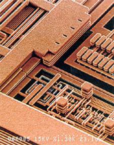
Figure 1. Scanning electron microscope image of IBM’s six-level copper interconnect technology (copyright IBM Corporation)

Advantages of Copper

Copper enables this by virtue of its superior electrical and thermal properties. As it is a better conductor of electricity than aluminium, copper interconnections can be made narrower - 0.1 microns instead of 0.25 microns. IBM says that the circuitry on the new chips will be built to dimensions of 0.2 microns, allowing for up to 12 million gates on a single chip. Altogether, CMOS 7S can pack 150-200 million transistors on a single chip, which translates as a big increase in computing power.

Implications of Smaller Chips

Such close packing is only possible because copper conducts heat very well, preventing damage to the circuits from overheating. Not that there is as much danger of that anyway - transistors based on the CMOS 7S technology operate at only 1.8 volts, allowing very low power operation. Devices based on the technology should be less of a drain on their batteries, or require less weighty power packs. Portable computers, mobile phones and personal digital assistants could all lose weight thanks to the copper-based chips.

Structure of the CMOS 7S Chips

As figure 2 shows, CMOS 7S is an intricate technology. Six layers of metal are laid down on each chip, allowing complex circuit design. But just how Sematech and IBM in particular managed to do this without poisoning the semiconductor remains a secret - understandably, given the massive potential market for devices based on copper technology.

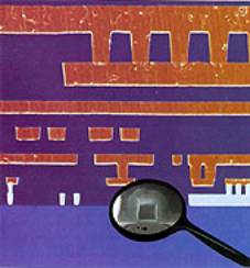
Figure 2. SEM cross-section of CMOS 7S copper process, showing the six copper levels used for chip wiring and one tungsten level for local interconnect. Inset shos 0.16 micron effective channel length, an impressive size reduction over current technology (copyright IBM Corporation)

Applications for the CMOS 7S Chips

IBM Microelectronics has already introduced its next generation of application-specific integrated circuits (ASICs) based on CMOS 7S. The company is also producing design tools and services to assist other electronics manufacturers in building their own products. Such design kits are aimed at helping developers of computers, communications equipment and consumer electronics improve the function of their products through the use of copper. The kits will enable the manufacture of ASICs designed to perform functions such as manipulating 3D graphics or controlling digital cameras. ASICs are already widely used to give computer intelligence to everything from electronic games to telephone switching systems.

Implications for the Copper Industry

So what will all this mean for the world consumption of copper? Unfortunately for the industry, not a lot. Despite the fact that millions of chips are sold each year and that this figure is expected to increase rapidly, the amount of copper material needed in each chip can be measured in the order of micrograms. But the prestige is important, according to Robert Payne, president of the Copper Development Association. ‘It’s the advanced technology provided by copper that is important,’ he said, ‘not the weight consumed.’

Copper Indium Diselenide as a Photovoltaic Material

Background

Although amorphous silicon is the leading thin-film photovoltaic (PV) material research is underway with other promising materials. Materials like Copper Indium Diselenide (CuInSe2 or CIS).
A Closer Look

The current world record thin-film solar cell efficiency of 17.7% is held by a device based on copper indium diselenide.

Researchers are studying routes for developing processes suitable for manufacturing to facilitate the deployment of copper indium diselenide technology. This work focuses on processes that are capable of being inexpensive while maintaining high performance. Four primary processes are being studied and the most promising will be chosen for further development. This research concentrates on the following four areas:

· Process development. Various deposition methods suitable for commercialising the CIS technology, including sublimation/evaporation, sputtering, electrodeposition, and spraying are being examined.

· In-situ junction formation. How to integrate the formation of the junction into the absorber fabrication process is being studied and has already demonstrated the feasibility of this concept with a nearly 10% efficient device that does not use cadmium sulfide.

· Substrate/back contact. The impact of the glass substrate and molybdenum contact on CIS-based solar cells as well as alternatives to glass/Mo designs are being studied.

· Capabilities Development. A more reliable Mo deposition system and a direct-current reactive ZnO process amenable to scale-up and fast deposition rates are being developed. These are essential to advancing CIS technology from the fundamental stage to pre-commercialisation.

Tuesday, September 26, 2006

Copper Alloys – Copper/Nickel/Tin Alloys

Background

Alloys with compositions in the range Cu-4Ni-4Sn to Cu-15Ni-8Sn harden by spinodal decomposition. This process is similar to a conventional age-hardening reaction but instead of a fine precipitate forming, periodic variations in composition develop in the crystal lattice. This leads to very considerable increases in strength without macroscopic distortion.
Key Properties

· Excellent elastic properties

· High resistance to stress relaxation
Applications
Electrical Contacts

These alloys are used for electrical contacts, particularly in very arduous applications such as telecommunications.

Copper Alloys - Copper Nickel Alloys

Background

Sometimes called cupro-nickels, there exists a range of different copper nickel alloys that possess different properties and hence are suited to a range of different applications. Some of the better known copper nickel alloys include:

· Copper with 10% nickel

· Copper with 30% nickel

· Copper with 25% nickel with 0.05-0.4% manganese

· Copper with 45% nickel (also known as constantan)

All copper nickel alloys consist of only one phase as the copper nickel binary system exhibits complete solid solubility.
Key Properties

Properties vary with composition, however, some properties are outlined below.

Copper 90/10 and Copper 70/30

· Outstanding resistance to corrosion, particularly sea water

· 70/30 is stronger and has superior resistance to impingement corrosion

· Good resistance to biofouling, with the 90/10 alloy being slightly superior compared to the 70/30 alloy

Copper rich alloys are:

· Ductile

· Can be hardened only by cold working

· Good corrosion resistance

· Good strength

· Low temperature co-efficient of electrical resistance

The nickel content in these alloys also enables them to retain their strength at elevated temperatures compared to copper alloys without nickel.
Applications
Sea Water Condensor Systems And Desalination Plants

Due to the good resistance to sea water corrosion, the 90/10 and 70/30 alloys are employed for sea water condenser systems and in desalination plants, as well as pipe work in chemical plants.
Automotive Applications

Due to the fact that the 90/10 alloy requires no surface protection and hence gives extra safety, this alloy is being increasingly employed for brake and hydraulic suspension systems and cooling systems in cars and commercial vehicles.
Marine Applications

The good resistance to biofouling and sea water corrosion resistance of the 90/10 and 70/30 alloys have lead to its use in applications such as cladding for ships’ hulls, legs of oil rig platforms and sea water intake screens.
Coins

The copper with 25% nickel with 0.05-0.4% manganese is commonly used for the manufacture of coins, medals and other semi valuable applications.
Resistance Wire

Due to the very low temperature co-efficient of electrical resistivity, the copper with 45% nickel alloy is used for resistance wire in high precision resistors. This property allows the resistor to operate at almost exactly the same resistance regardless of temperature.
Thermocouples

The copper-45% nickel alloy is also used for thermocouples as it develops a high and uniform EMF when coupled with other metals such as copper and iron.
Other Applications

Cooling circuits, ammunition, sea water corrosion-resistant assemblies, condenser tubes.

Monday, September 25, 2006

Copper Alloys Copper C101 Properties, Fabrication and Applications, Supplier Data by Aalco

Background

It is believed that copper has been mined for over 5000 years. It can be found in elemental form and in the minerals cuprite, malachite, azurite, chalcopyrite and bornite. Copper is also often found as a by-product of silver production.

Basic Copper Properties

Next to silver, copper is the next best conductor. It is a yellowish red metal that polishes to a bright metallic lustre. It is tough, ductile and malleable. Copper has a disagreeable taste and a peculiar smell.

Copper is resistant to corrosion in most atmospheres including marine and industrial environments. It is corroded by oxidising acids, halogens, sulphides and ammonia based solutions.

Alloy C101

C101 is the designation for moderate copper used in engineering applications.

High ductility and impact strength also serve to make an extremely useful material.

C101 is the base material that common brasses and bronzes are produced from.

High Conductivity Copper

C101 is also known as HC or high conductivity copper. It has a nominal conductivity of 100% IACS (International Annealed Copper Standard). C101 also has high thermal conductivity. C101 is therefore the material of choice for use in conductors and electrical components but not when the service environment is a reducing atmosphere.

Chemical Composition

Table 1. Typical chemical composition for copper alloy C101

%

C101

Cu

99.9 min

Pb

-

Sn

-

Fe

-

Al

-

Mn

-

Zn

-

Si

-

Ni

-

P

-

Properties

Mechanical Properties

Table 2. Typical mechanical properties for copper alloy C101

Grade

C101

Tensile Strength (MPa)

200-360

Proof Stress 0.2% (MPa)

50-340

Elongation A5 (%)

42

Hardness VPN

40

Physical Properties

Table 3. Typical physical properties for copper alloy C101

Property

Value

Density

8.91 g/cm3

Melting Point

1083 °C

Modulus of Elasticity

117 GPa

Electrical Resistivity

0.0171x10⁻⁶ Ω.m

Thermal Conductivity

391.1 W/m.K at 100°C

Thermal Expansion

16.9x10⁻⁶ /K at 100°C

Alloy Designations

HC copper corresponds to the following designations:

CEN

BS

UNS

ISO

CW004A

C101

C11000

Cu-ETP

Corrosion Resistance

Corrosion resistance is either good or excellent in most environments and atmospheres other than those containing ammonia ions.

Fabrication

Cold Working

C101 can be readily cold worked. When in the annealed condition, it can be readily bent to shape and has excellent ductility.

It work hardens relatively slowly and can be annealed in neutral or oxidising atmospheres.

Hot Working

C101 is very readily hot worked.

Heat Treatment

Solution treatment or annealing can be done by rapid cooling after heating to 370-650°C.


Machinability

C101 has a machinability rating of 20 when Alloy 360 FC Brass is 100.

Welding

Soldering of C101 is excellent. Brazability and butt welding are also rated as good. Gas shielded arc welding has a fair rating. All other welding processes are not recommended.

Applications

C101 is typically used in:

· General engineering

· Electronics

· Automotive

· Domestic Appliances

· Cold formed components

Copper Alloys Copper C106 Properties, Fabrication and Applications, Supplier Data by Aalco

Background

It is believed that copper has been mined for over 5000 years. It can be found in elemental form and in the minerals cuprite, malachite, azurite, chalcopyrite and bornite. Copper is also often found as a by-product of silver production.

Basic Copper Properties

Next to silver, copper is the next best conductor. It is a yellowish red metal that polishes to a bright metallic lustre. It is tough, ductile and malleable. Copper has a disagreeable taste and a peculiar smell.

Copper is resistant to corrosion in most atmospheres including marine and industrial environments. It is corroded by oxidising acids, halogens, sulphides and ammonia based solutions.

Alloy C106

C106 is phosphorous de-oxidised non-arsenical copper that is 99.85% pure.

Chemical Composition

Table 1. Typical chemical composition for copper alloy C106

%

C106

Cu

99.85 min

Pb

-

Sn

-

Fe

-

Al

-

Mn

-

Zn

-

Si

-

Ni

-

P

0.015-0.04

Properties

Mechanical Properties

Table 2. Typical mechanical properties for copper alloy C106

Grade

C106

Tensile Strength (MPa)

220

Proof Stress 0.2% (MPa)

45

Elongation A5 (%)

45

Hardness VPN

45-60

Physical Properties

Table 3. Typical physical properties for copper alloy C106

Property

Value

Density

8.94 g/cm3

Melting Point

1083°C

Modulus of Elasticity

GPa

Electrical Resistivity

0.0203x10⁻⁶ Ω.m

Thermal Conductivity

339.2 W/m.K at 100°C

Thermal Expansion

16.9x10⁻⁶ /K at 100°C

Alloy Designations

Phosphorous de-oxidised non-arsenical copper corresponds to the following standard designations and specifications:

CEN

BS

UNS

ISO

CW024A

C106

C12200

Cu-DHP

Corrosion Resistance

Corrosion resistance is either good or excellent in most environments and atmospheres other than those containing ammonia ions.

Fabrication

Cold Working

C106 has an excellent response to cold working.

Hot Working

With forging of brass rated as 100, the hot forgeability of C106 is rated at 65. Hot working temperatures should be between 760 and 870°C

Heat Treatment

Solution treatment or annealing can be done by rapid cooling after heating to 370-650°C.

Machinability

This alloy has a machinability rating of 20 when Alloy 360 FC Brass is 100.

Welding

Deoxidation of C106 improves embrittlement resistance during welding.

Brazing and soldering are both excellent joining methods for C106. Gas shielded arc welding is also excellent. Oxyacetylene welding and butt welding are good. Welding methods not recommended include:

· Coated metal arc welding

· Spot welding

· Seam welding

Applications

C106 is typically used in applications like:

· Refrigeration

· Gutters and roofing

· Gas plants

· Busbars

· Hydraulic, air and oil lines

· Air Conditioning and refrigeration

· Heater units and burners tubes Consumer

· Plumbing pipe and fittings